Superconducting qubits
Superconducting circuits are the leading solid-state platform for quantum computing, and their coherence is limited by the qubit’s microscopic environment: two-level-system defects in materials and interfaces, and the phonons that these defects and the qubit itself can emit. We treat the qubit, its defect bath and its phonon bath as one coupled electromechanical system, build microscopic models of how each limits coherence, and use them to engineer compact qubits with longer lifetimes.
Recent topics
-
Phonon-protected superconducting qubits
The two-level-system defects that limit qubit coherence lose energy by emitting phonons. Embedding qubits in phononic-bandgap metamaterials suppresses this emission, and we co-design compact qubits with phononic crystals so that neither the defects nor the phonon environment offers the qubit a channel to decay.
-
Merged-element transmons and compact circuits
In a merged-element transmon, the Josephson junction also serves as the qubit's capacitor, shrinking the qubit's footprint by orders of magnitude. We develop these compact qubits and new circuit architectures built from Josephson junctions.
-
Two-level systems in Josephson junctions
A small junction contains only a few two-level-system defects, which can be detected and tracked one by one. We count these defects across junction sizes and fabrication processes, tune individual defects with strain, and test the standard tunneling model of two-level systems over a wide range of frequencies.
-
Microscopic origins of dielectric loss
As surface loss improves, defects inside the substrate start to limit qubit lifetimes. We identify specific defects, such as boron acceptors in silicon, that act as two-level-system baths, and set purity requirements for qubit substrates.
-
Interface piezoelectric loss
Silicon is not piezoelectric, but the broken symmetry at aluminum–silicon interfaces creates a weak piezoelectric response. We measure the loss this causes in qubits and predict that it overtakes two-level-system loss at high qubit frequencies.
-
Van der Waals materials for superconducting circuits
Crystalline van der Waals materials such as hBN and NbSe₂ offer circuit elements free of amorphous oxides. We build superconducting circuits from these materials, and use microwave resonators as contactless probes of two-dimensional superconductors.
In collaboration with Feng Wang
Research highlights
-
arXiv 2026
Interface Piezoelectric Loss in Superconducting Qubits
Superconducting qubits on silicon have a previously unrecognized loss channel: they radiate phonons through a weak piezoelectric response at the aluminum–silicon interface. We measure this loss in a transmon embedded in a surface acoustic wave resonator and predict that it overtakes two-level-system loss at high qubit frequencies.
Read the paper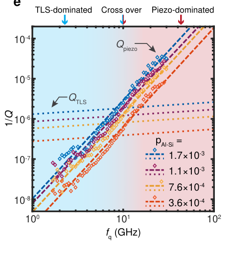
-
Nature Communications 2026
Observation of interface piezoelectricity in superconducting devices on silicon
Bulk silicon is not piezoelectric, but the broken symmetry at aluminum–silicon interfaces produces a piezoelectric response that we detect from room temperature down to millikelvin temperatures. This effect, predicted decades ago and observed here for the first time in superconducting devices, is a significant surface loss channel for superconducting qubits.
Read the paper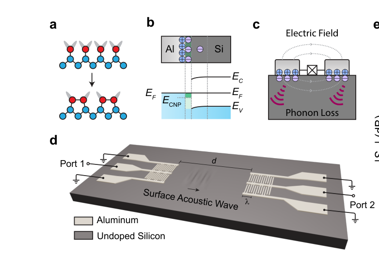
-
Nature Physics 2025
Non-Markovian dynamics of a superconducting qubit in a phononic bandgap
Embedding a transmon qubit in a phononic-bandgap metamaterial suppresses phonon emission by the two-level-system defects it couples to, driving the qubit’s dissipation into a non-Markovian regime. Co-designing the phonon environment opens a path to qubits that are both smaller and longer-lived.
Read the paper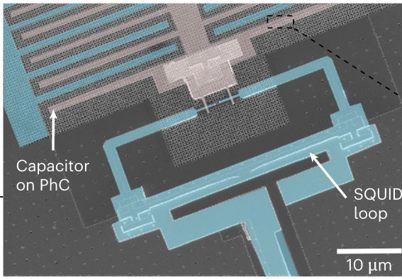
-
Physical Review X 2024
Acceptor-Induced Bulk Dielectric Loss in Superconducting Circuits on Silicon
Boron acceptors in silicon behave like two-level systems, and even part-per-billion concentrations of boron in the substrate are enough to make superconducting qubits decay. By measuring resonators on silicon wafers with different boron concentrations, we give the first detailed microscopic picture of a two-level-system bath and show that substrate purity is critical for next-generation superconducting quantum processors.
Read the paper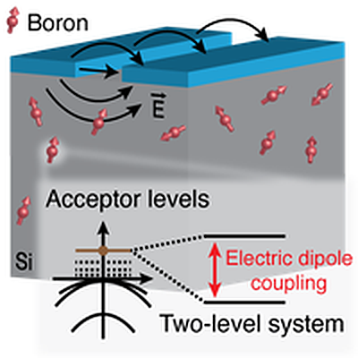
Recent group publications on superconducting qubits
-
Nature Materials (2026) News & Views
@article{ahn_taking_2026, title = {Taking the heat off tantalum}, url = {https://www.nature.com/articles/s41563-026-02766-5}, doi = {10.1038/s41563-026-02766-5}, journal = {Nature Materials}, issn = {1476-1122, 1476-4660}, author = {Ahn, Tae Gyu and Sipahigil, Alp}, month = oct, year = {2026} } -
arXiv:2605.15554 (2026)
@unpublished{zhou_interface_2026,
  title = {Interface {Piezoelectric} {Loss} in {Superconducting} {Qubits}},
  url = {http://arxiv.org/abs/2605.15554},
  doi = {10.48550/arXiv.2605.15554},
  author = {Zhou, Haoxin and Yu, Kangdi and Balaji, Yashwanth and Shirol, Sanjit and Sementilli, Leo and Zhang, Zi-Huai and Schwartzberg, Adam and Sipahigil, Alp},
  month = may,
  year = {2026},
  note = {arXiv:2605.15554 [quant-ph]},
  arxiv = {2605.15554}
}
Dissipation remains a central obstacle to improving superconducting quantum circuits, yet the microscopic origins of loss in widely used materials platforms are not fully understood. Here, we report the observation of interface piezoelectricity-induced dissipation in superconducting qubits fabricated on high-resistivity silicon. Our devices use a transmon qubit with a shunt capacitor that simultaneously serves as an interdigital transducer embedded in a surface acoustic wave resonator. By tuning the qubit transition into resonance with discrete mechanical modes, we observe up to a factor-of-two reduction in qubit lifetime, consistent with energy exchange between the qubit and mechanical modes mediated by piezoelectric coupling at the aluminum-silicon interface. Our findings provide direct evidence for interface piezoelectricity as a distinct loss channel in superconducting qubits. Combined with multiphysics simulations, these findings suggest that interface piezoelectric loss can dominate over loss from two-level systems at sufficiently high frequencies.
-
Nature Communications 17, 377 (2026)
@article{zhou_observation_2026,
  title = {Observation of interface piezoelectricity in superconducting devices on silicon},
  volume = {17},
  url = {https://doi.org/10.1038/s41467-025-67066-z},
  doi = {10.1038/s41467-025-67066-z},
  journal = {Nature Communications},
  pages = {377},
  author = {Zhou, H. and Li, E. and Godeneli, K. and Zhang, Z.-H. and Jahanbani, S. and Yu, K. and Odeh, M. and Aloni, S. and Griffin, S. and Sipahigil, A.},
  year = {2026},
  arxiv = {2409.10626}
}
The development of superconducting quantum processors relies on understanding and mitigating decoherence in superconducting qubits. Piezoelectric coupling contributes to decoherence by mediating energy exchange between microwave photons and acoustic phonons. Although bulk centrosymmetric materials like silicon and sapphire are non-piezoelectric and commonly used as qubit substrates, the lack of centrosymmetry at interfaces may induce piezoelectric losses. This effect was predicted decades ago but never experimentally observed in superconducting devices. Here, we report interface piezoelectricity at aluminum-silicon junctions and demonstrate it as a significant loss channel in superconducting devices. Using aluminum interdigital transducers on silicon, we observe piezoelectric transduction from room to millikelvin temperatures, with an effective electromechanical coupling factor K 2 ≈ (3 ± 0.4) × 10 −5 %, comparable to weakly piezoelectric substrates. Modeling shows this mechanism limits qubit quality factors to Q 10 4 − 10 8 , depending on surface participation and mode matching. These findings reveal interface piezoelectricity as a major dissipation channel and highlight the need for heterostructure and phononic engineering in next-generation superconducting qubits.
-
Nature Physics 21, 406–411 (2025)
@article{odeh_non-markovian_2025,
  title = {Non-{Markovian} dynamics of a superconducting qubit in a phononic bandgap},
  volume = {21},
  url = {https://www.nature.com/articles/s41567-024-02740-5},
  doi = {10.1038/s41567-024-02740-5},
  journal = {Nature Physics},
  number = {3},
  pages = {406--411},
  issn = {1745-2473, 1745-2481},
  author = {Odeh, Mutasem and Godeneli, Kadircan and Li, Eric and Tangirala, Rohin and Zhou, Haoxin and Zhang, Xueyue and Zhang, Zi-Huai and Sipahigil, Alp},
  month = mar,
  year = {2025},
  arxiv = {2312.01031}
}
The overhead to construct a logical qubit from physical qubits rapidly increases with the decoherence rate. Current superconducting qubits reduce dissipation due to two-level systems (TLSs) by using large device footprints. However, this approach provides partial protection, and results in a trade-off between qubit footprint and dissipation. This work introduces a new platform using phononics to engineer superconducting qubit-TLS interactions. We realize a superconducting qubit on a phononic bandgap metamaterial that suppresses TLS-mediated phonon emission. We use the qubit to probe its thermalization dynamics with the phonon-engineered TLS bath. Inside the phononic bandgap, we observe the emergence of non-Markovian qubit dynamics due to the Purcell-engineered TLS lifetime of 34 μs. We discuss the implications of these observations for extending qubit relaxation times through simultaneous phonon protection and miniaturization.
-
Physical Review X 14, 041022 (2024)
@article{zhang_acceptor-induced_2024,
  title = {Acceptor-{Induced} {Bulk} {Dielectric} {Loss} in {Superconducting} {Circuits} on {Silicon}},
  volume = {14},
  url = {https://link.aps.org/doi/10.1103/PhysRevX.14.041022},
  doi = {10.1103/PhysRevX.14.041022},
  journal = {Physical Review X},
  number = {4},
  pages = {041022},
  issn = {2160-3308},
  author = {Zhang, Zi-Huai and Godeneli, Kadircan and He, Justin and Odeh, Mutasem and Zhou, Haoxin and Meesala, Srujan and Sipahigil, Alp},
  month = oct,
  year = {2024},
  arxiv = {2402.17155}
}
The performance of superconducting quantum circuits is primarily limited by dielectric loss due to interactions with two-level systems (TLSs). State-of-the-art circuits with engineered material interfaces are approaching a limit where dielectric loss from bulk substrates plays an important role. However, a microscopic understanding of dielectric loss in crystalline substrates is still lacking. In this work, we show that boron acceptors in silicon constitute a TLS bath that leads to an energy dissipation channel for superconducting circuits. We discuss how the electronic structure of boron acceptors leads to an effective TLS response in silicon. We sweep the boron concentration in silicon and demonstrate the bulk dielectric loss limit from boron acceptors. We show that boron-induced dielectric loss can be reduced in a magnetic field due to the spin-orbit structure of boron. This work provides the first detailed microscopic description of a TLS bath for superconducting circuits and demonstrates the need for ultrahigh-purity substrates for next-generation superconducting quantum processors. Published by the American Physical Society 2024
* Equal contribution