Aug 1
2026
Zihuai, Haoxin, and Hong start faculty positions!
Congratulations to our newest group alumni!!! You can read more about their research labs:
The Sipahigil Lab at UC Berkeley and Berkeley Lab studies the materials and device physics that limit solid-state quantum hardware performance, and uses this understanding to engineer longer coherence, lower errors and scalable interconnects.
Superconducting circuits are the leading solid-state platform for quantum computing, and their error rates are set largely by decoherence. We study how superconducting qubits lose coherence to defects and phonons, and engineer these interactions to build qubits with longer coherence and lower error rates.
Quantum hardware, like its classical counterparts, needs interconnects between processing, memory and communication modules. We use emerging materials and new device architectures to develop high-fidelity quantum transducers between electrical, mechanical, spin and optical quantum states.
Defects in silicon can act as artificial atoms with telecom-band optical transitions and long-lived spins. We engineer these defects in silicon photonics to build scalable, optically interconnected quantum network nodes.
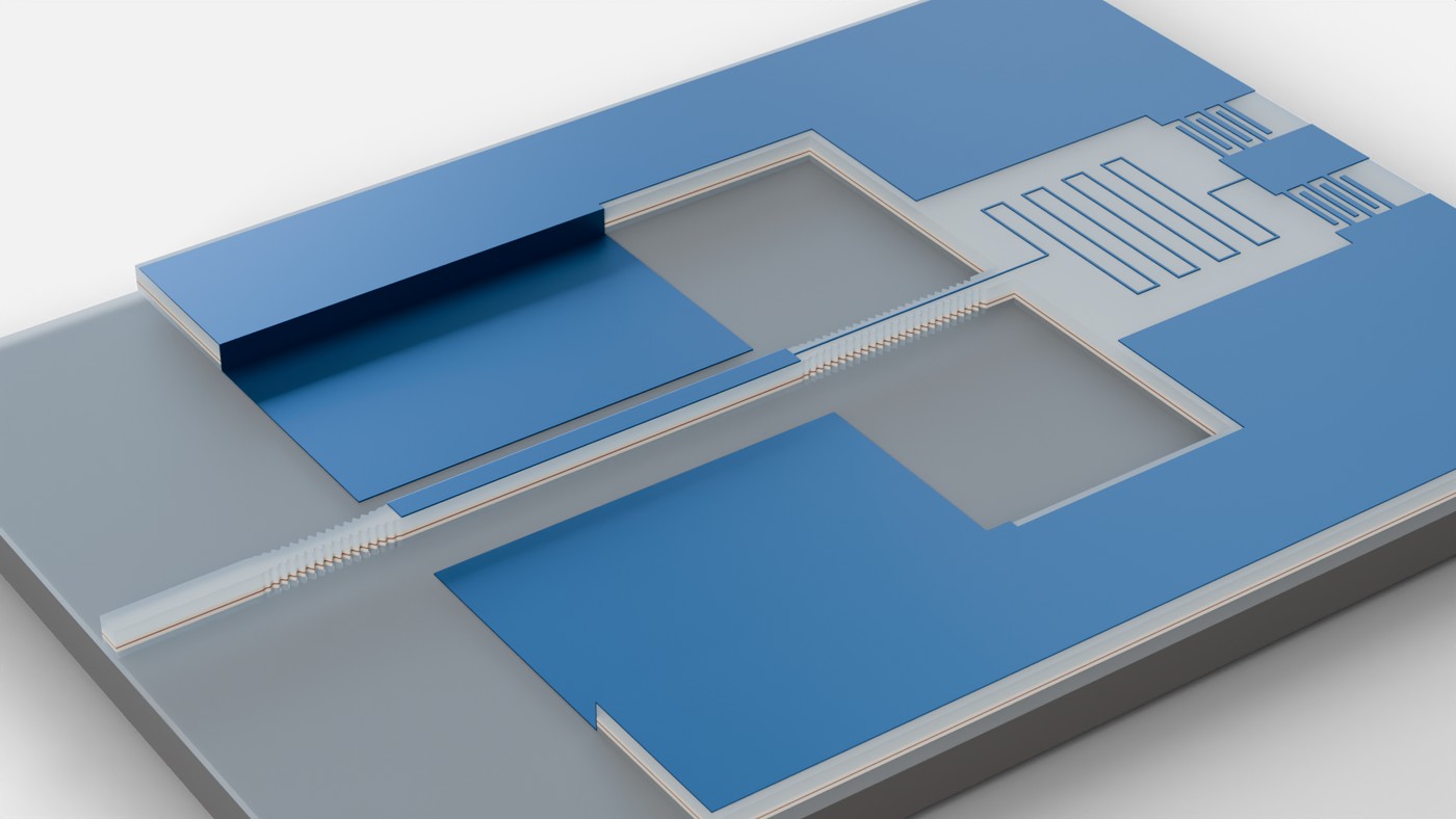
Microwave-optical quantum transducers are limited by the weak electro-optic nonlinearity of conventional materials. We propose a transducer built on quantum-well excitons, whose optical resonance shifts strongly in a microwave electric field through the quantum-confined Stark effect. Strong coupling to an optical cavity turns the excitons into polaritons with a vacuum electro-optic coupling up to five orders of magnitude larger than in thin-film lithium niobate.
Read the paper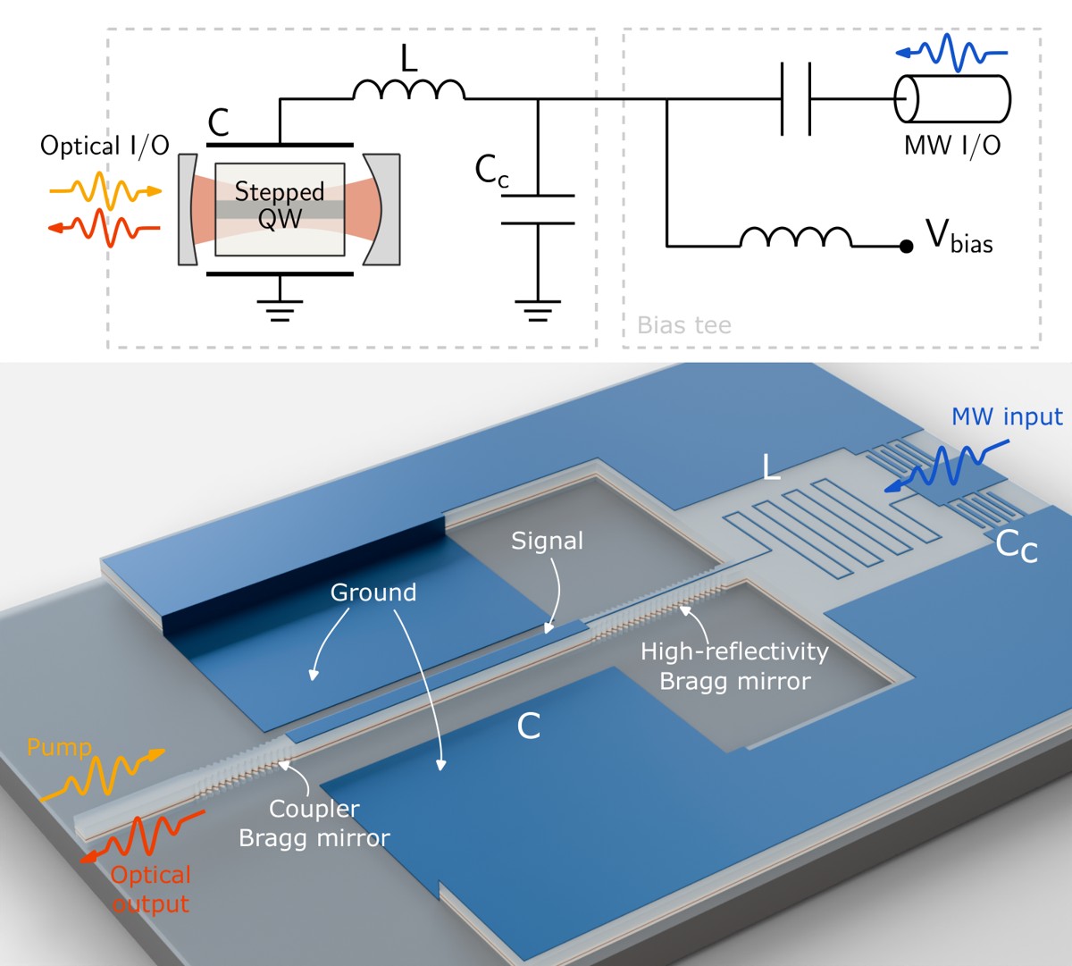
Superconducting qubits on silicon have a previously unrecognized loss channel: they radiate phonons through a weak piezoelectric response at the aluminum–silicon interface. We measure this loss in a transmon embedded in a surface acoustic wave resonator and predict that it overtakes two-level-system loss at high qubit frequencies.
Read the paper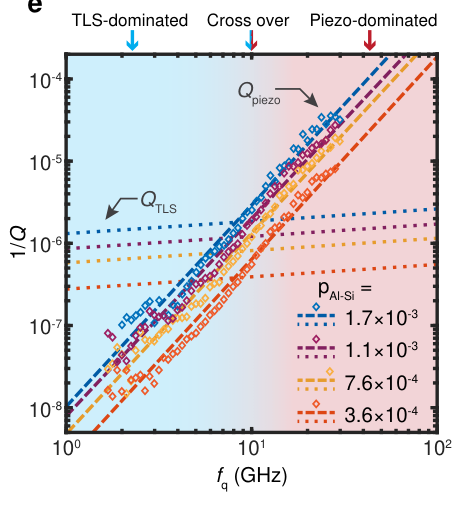
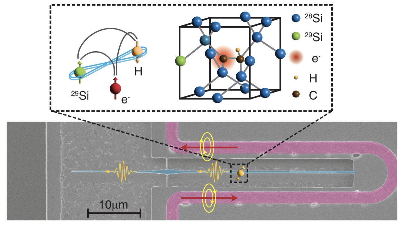
We realize a three-qubit register in silicon photonics from the electron spin of a T center and two nearby nuclear spins, with nuclear-spin coherence times up to 112 ms and entangling gates between the nuclear spins. Combined with the T center’s telecom-band optical interface, these are key ingredients for a scalable quantum network node in silicon.
Read the paper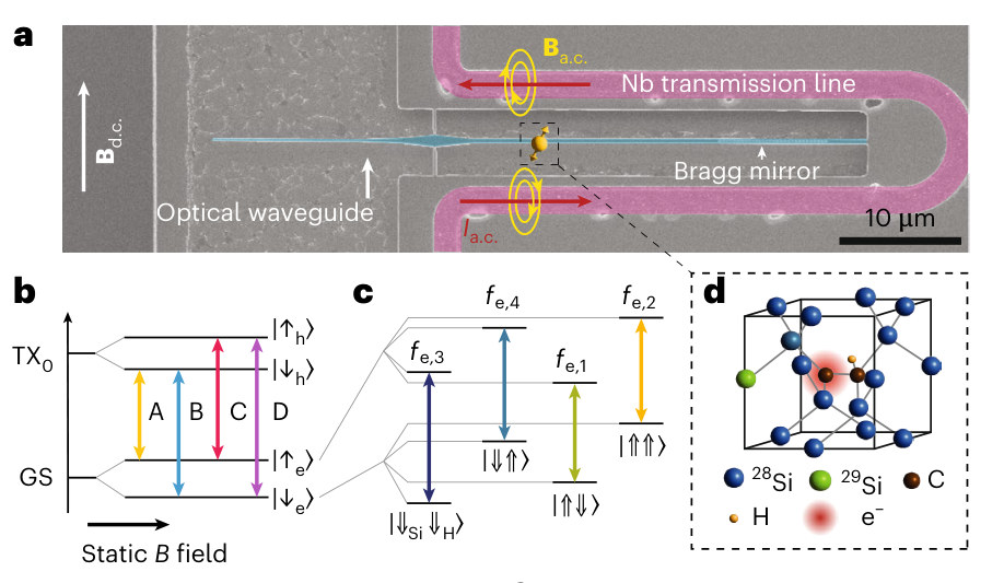
Bulk silicon is not piezoelectric, but the broken symmetry at aluminum–silicon interfaces produces a piezoelectric response that we detect from room temperature down to millikelvin temperatures. This effect, predicted decades ago and observed here for the first time in superconducting devices, is a significant surface loss channel for superconducting qubits.
Read the paper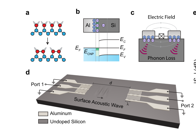
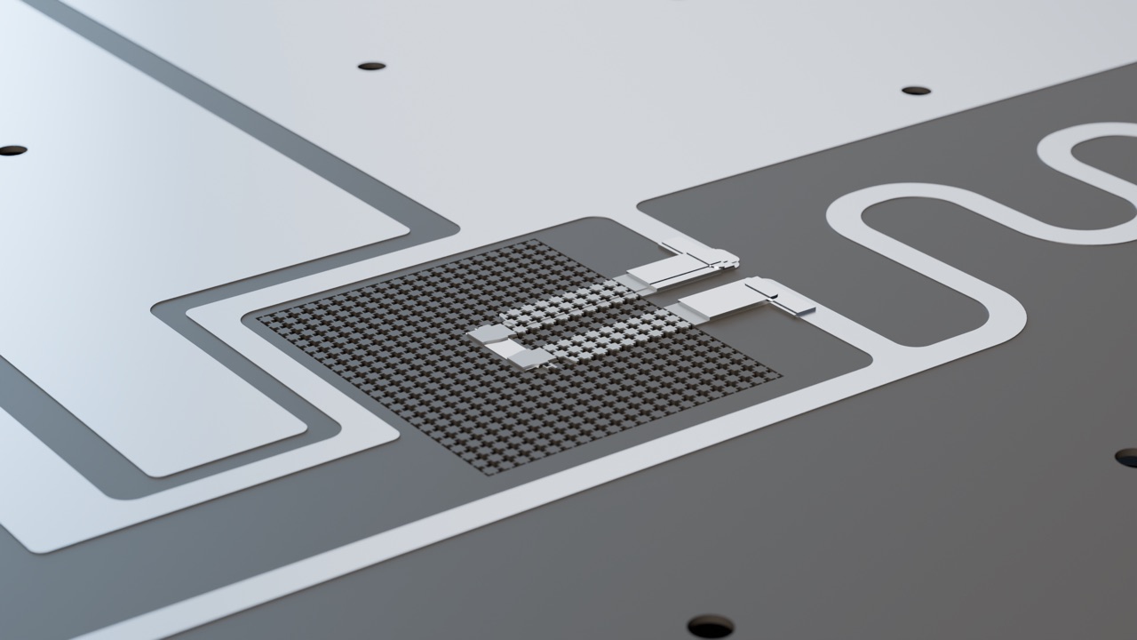
Embedding a transmon qubit in a phononic-bandgap metamaterial suppresses phonon emission by the two-level-system defects it couples to, driving the qubit’s dissipation into a non-Markovian regime. Co-designing the phonon environment opens a path to qubits that are both smaller and longer-lived.
Read the paper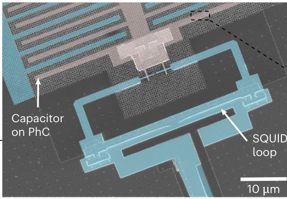
Boron acceptors in silicon behave like two-level systems, and even part-per-billion concentrations of boron in the substrate are enough to make superconducting qubits decay. By measuring resonators on silicon wafers with different boron concentrations, we give the first detailed microscopic picture of a two-level-system bath and show that substrate purity is critical for next-generation superconducting quantum processors.
Read the paper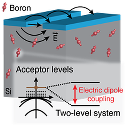
@unpublished{yama_microwave-optical_2026,
  title = {Microwave-optical quantum transduction with quantum-well exciton polaritons},
  url = {http://arxiv.org/abs/2611.21785},
  doi = {10.48550/arXiv.2611.21785},
  author = {Yama, Nicholas S. and Khalifa, Mohammad and Wei, Yuxuan and Gupta, Adbhut and Pfeiffer, Loren N. and Wang, Feng and Sipahigil, Alp},
  month = nov,
  year = {2026},
  note = {arXiv:2611.21785 [quant-ph]},
  arxiv = {2611.21785}
}
Linking superconducting quantum processors over optical fiber requires microwave-optical quantum transducers that are efficient, high-bandwidth, and low-noise. This combination has been out of reach because of the weak nonlinearities of conventional electro-optic (EO) materials. We propose a transducer with an engineered, strong EO nonlinearity using the quantum-confined Stark effect (QCSE) of quantum-well excitons. The QCSE transducer leverages the strong light-matter interactions and extreme polarizability of quantum well excitons. Strong coupling to an optical cavity forms exciton-polaritons whose vacuum EO coupling is up to five orders of magnitude larger than in a typical thin-film lithium niobate device. We describe a GaAs/AlGaAs stepped-quantum-well transducer design with predicted transduction efficiencies above 60% and fewer than 0.01 added noise quanta over a 60 MHz bandwidth, using pump powers below 10 μW and loaded optical and microwave quality factors of only 3×10⁴ and 10³. We further show that the cavity protection of the polariton provides robustness against inhomogeneous broadening of the quantum well excitons.
@article{ahn_taking_2026,
  title = {Taking the heat off tantalum},
  url = {https://www.nature.com/articles/s41563-026-02766-5},
  doi = {10.1038/s41563-026-02766-5},
  journal = {Nature Materials},
  issn = {1476-1122, 1476-4660},
  author = {Ahn, Tae Gyu and Sipahigil, Alp},
  month = oct,
  year = {2026}
}
@unpublished{zhang_resolving_2026,
  title = {Resolving and resetting the charge environment of single T-centers in silicon p-i-n waveguides},
  url = {https://arxiv.org/abs/2608.15993},
  doi = {10.48550/ARXIV.2608.15993},
  author = {Zhang, Chaoshen and Song, Hanbin and Komza, Lukasz and Day, Aaron M. and Garcia, Enrique and Witt, Donald and Bhaskar, Mihir K. and Sipahigil, Alp and Hu, Evelyn L.},
  month = aug,
  year = {2026},
  note = {Version Number: 1},
  arxiv = {2608.15993}
}
The silicon T-center is a telecom-band spin-photon interface in a manufacturable photonics platform. In nanophotonic devices, however, its optical linewidth is broadened by a fluctuating charge environment, limiting photon indistinguishability for quantum networking. Here, we address this challenge through characterization and suppression of the local charge-noise of single T-centers in lateral p-i-n waveguides, demonstrating an unheralded method of T-center optical linewidth narrowing. Above-band illumination resets the charge environment, neutralizing the local field and suppressing spectral diffusion. Across 46 emitters this reset narrows the median linewidth 3.5-fold to 0.57(11) GHz, and an optimized emitter reaches 128(22) MHz, the narrowest unheralded linewidth reported for an integrated T-center. The narrowed transition supports coherent optical Rabi oscillations with a coherence time of 20(2) ns. Finally, we perform Stark-shift tuning using the p-i-n junction, and read out the local electric field and the charge-noise width at 15 mK. An analytical model of proximal surfaces, bulk, and junction field effects provides good agreement with our findings. Our multi-pronged characterization of the nanophotonic-integrated T-center charge environment enables future device optimization toward scalable quantum interconnects.
@article{zhu_point_2026,
  title = {Point defects in semiconductors: {Friends} and foes for quantum technologies},
  volume = {51},
  url = {https://link.springer.com/10.1557/s43577-026-01095-x},
  doi = {10.1557/s43577-026-01095-x},
  journal = {MRS Bulletin},
  number = {5},
  pages = {615--629},
  issn = {0883-7694, 1938-1425},
  author = {Zhu, Yizhi and Zhang, Zi-Huai and Chen, Weiru and Sakib, Mashnoon Alam and Weber-Bargioni, Alexander and Griffin, Sinéad and Raja, Archana and Sipahigil, Alp and Hautier, Geoffroy},
  month = may,
  year = {2026}
}
Point defects in semiconductors are both a curse and a blessing in microelectronics: they enable the control of electrical conductivity through doping, yet can also act as trapping and recombination centers that degrade device performance. In quantum information science, defects play a similarly dual role. They can be harnessed as spin–photon interfaces enabling the coupling of electronic and nuclear spins to light and the creation of distributed entanglement for quantum networks or used as atomistic scale sensors for quantum sensing. At the same time, defects are a major source of decoherence for superconducting qubits, one of the leading quantum computing platforms. This article discusses how a deeper materials-level understanding of defects can guide the design of improved quantum devices for communication, sensing, and computation.
Congratulations to our newest group alumni!!! You can read more about their research labs:
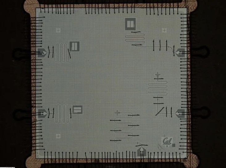
In Fall 2025, 30 students in 10 teams took the first offering of EE290, Superconducting Quantum Circuits (aka “Quantum Tapeout”). Each team designed its own superconducting qubit chip, and in December the students tested their fabricated chips, measuring qubit lifetimes, readout resonator frequencies and dispersive …
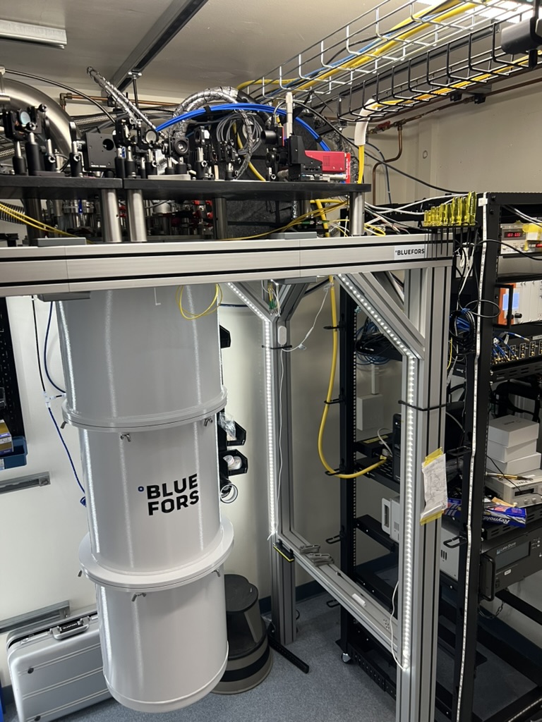
Our microwave and optics labs had two big upgrades!