Optically interconnected spin-qubits in silicon photonics
Silicon hosts optically active defects, artificial atoms that emit in the telecom O-band and can be created with CMOS-compatible processing in silicon photonics. The T center combines this telecom optical interface with electron and nuclear spin memories. We engineer these emitters, integrate them into silicon photonic circuits, and work toward quantum network nodes that distribute entanglement over optical fiber.
Recent topics
-
How can we engineer an atom-like qubit in silicon?
Few defects in silicon combine bright telecom-band optical transitions with long-lived spins. We use first-principles calculations to find and characterize defects like the T center, and to understand what makes a defect optically active.
In collaboration with Geoffroy Hautier
Materials for Quantum Technology 2024Science Advances 2023Physical Review Materials 2022
-
Indistinguishable photons from scalable cavity arrays
Quantum networks need identical photons from many emitters on one chip. We integrate G and T centers into silicon photonic waveguides, cavities and bus-coupled cavity arrays that address many emitters at once.
-
Understanding and reducing spectral diffusion
Single T centers in nanophotonic devices have much broader optical lines than in bulk silicon, and every network application depends on narrowing them. We study the fluctuating charge environment behind this spectral diffusion and test ways to reduce it, from new materials and fabrication routes to electrical control of the charge environment.
In collaboration with Evelyn Hu
-
Multi-qubit registers based on nuclear spins
Nuclear spins near a T center can store quantum information for long times. We build registers from a T center's electron spin and nearby nuclear spins, with entangling gates between the nuclear spins, as the memory of a quantum repeater node.
Research highlights
-
Nature Nanotechnology 2026
Entanglement of a nuclear spin qubit register in silicon photonics
We realize a three-qubit register in silicon photonics from the electron spin of a T center and two nearby nuclear spins, with nuclear-spin coherence times up to 112 ms and entangling gates between the nuclear spins. Combined with the T center’s telecom-band optical interface, these are key ingredients for a scalable quantum network node in silicon.
Read the paper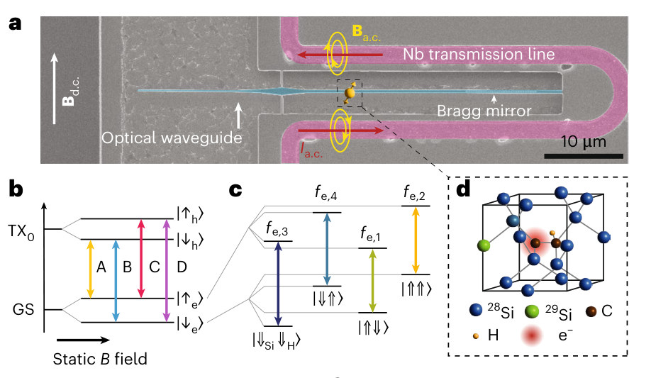
-
Optica 2025
Multiplexed color centers in a silicon photonic cavity array
We build arrays of photonic crystal cavities coupled to a common silicon bus waveguide, giving simultaneous access to individually addressable, cavity-enhanced T centers. We demonstrate frequency-multiplexed operation of two T centers in separate cavities, a route to efficient on-chip and long-distance entanglement distribution.
Read the paper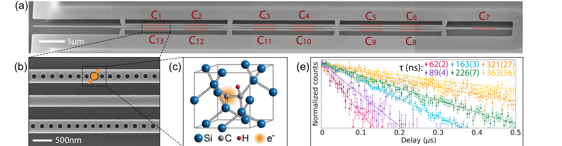
-
PRX Quantum 2025
Laser-Induced Spectral Diffusion of T Centers in Silicon Nanophotonic Devices
T centers in silicon nanophotonic devices have broadened optical lines, a challenge for generating indistinguishable photons. By tracking the optical frequency of single T centers in a photonic crystal cavity from nanoseconds to milliseconds, we find that the line is stable in the dark and identify laser-induced processes as the dominant source of spectral diffusion.
Read the paper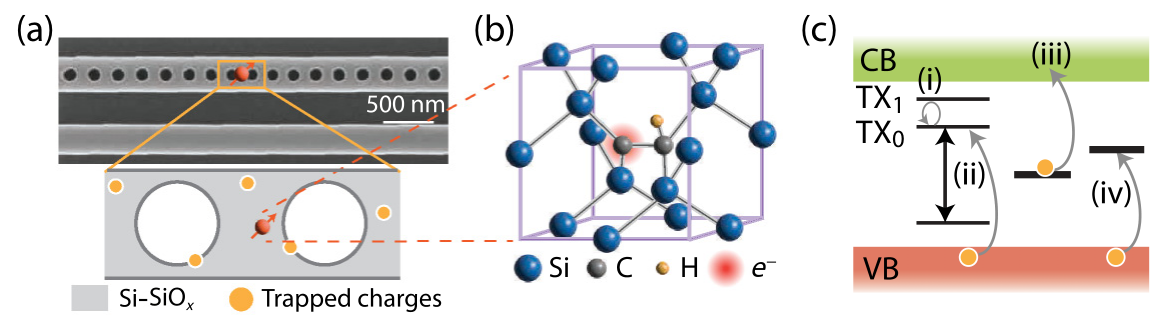
-
Nature Communications 2024
Indistinguishable photons from an artificial atom in silicon photonics
A G center, an artificial atom in a silicon waveguide, emits high-purity single photons in the telecom O-band. Using time-delayed two-photon interference, we show that these photons are indistinguishable, establishing artificial atoms in silicon photonics as quantum light sources for photonic quantum networks and processors.
Read the paper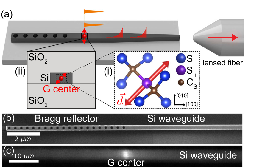
Recent group publications on spin qubits in silicon photonics
-
arXiv:2608.15993 (2026)
@unpublished{zhang_resolving_2026,
  title = {Resolving and resetting the charge environment of single T-centers in silicon p-i-n waveguides},
  url = {https://arxiv.org/abs/2608.15993},
  doi = {10.48550/ARXIV.2608.15993},
  author = {Zhang, Chaoshen and Song, Hanbin and Komza, Lukasz and Day, Aaron M. and Garcia, Enrique and Witt, Donald and Bhaskar, Mihir K. and Sipahigil, Alp and Hu, Evelyn L.},
  month = aug,
  year = {2026},
  note = {Version Number: 1},
  arxiv = {2608.15993}
}
The silicon T-center is a telecom-band spin-photon interface in a manufacturable photonics platform. In nanophotonic devices, however, its optical linewidth is broadened by a fluctuating charge environment, limiting photon indistinguishability for quantum networking. Here, we address this challenge through characterization and suppression of the local charge-noise of single T-centers in lateral p-i-n waveguides, demonstrating an unheralded method of T-center optical linewidth narrowing. Above-band illumination resets the charge environment, neutralizing the local field and suppressing spectral diffusion. Across 46 emitters this reset narrows the median linewidth 3.5-fold to 0.57(11) GHz, and an optimized emitter reaches 128(22) MHz, the narrowest unheralded linewidth reported for an integrated T-center. The narrowed transition supports coherent optical Rabi oscillations with a coherence time of 20(2) ns. Finally, we perform Stark-shift tuning using the p-i-n junction, and read out the local electric field and the charge-noise width at 15 mK. An analytical model of proximal surfaces, bulk, and junction field effects provides good agreement with our findings. Our multi-pronged characterization of the nanophotonic-integrated T-center charge environment enables future device optimization toward scalable quantum interconnects.
-
MRS Bulletin 51, 615–629 (2026)
@article{zhu_point_2026,
  title = {Point defects in semiconductors: {Friends} and foes for quantum technologies},
  volume = {51},
  url = {https://link.springer.com/10.1557/s43577-026-01095-x},
  doi = {10.1557/s43577-026-01095-x},
  journal = {MRS Bulletin},
  number = {5},
  pages = {615--629},
  issn = {0883-7694, 1938-1425},
  author = {Zhu, Yizhi and Zhang, Zi-Huai and Chen, Weiru and Sakib, Mashnoon Alam and Weber-Bargioni, Alexander and Griffin, Sinéad and Raja, Archana and Sipahigil, Alp and Hautier, Geoffroy},
  month = may,
  year = {2026}
}
Point defects in semiconductors are both a curse and a blessing in microelectronics: they enable the control of electrical conductivity through doping, yet can also act as trapping and recombination centers that degrade device performance. In quantum information science, defects play a similarly dual role. They can be harnessed as spin–photon interfaces enabling the coupling of electronic and nuclear spins to light and the creation of distributed entanglement for quantum networks or used as atomistic scale sensors for quantum sensing. At the same time, defects are a major source of decoherence for superconducting qubits, one of the leading quantum computing platforms. This article discusses how a deeper materials-level understanding of defects can guide the design of improved quantum devices for communication, sensing, and computation.
-
Nature Nanotechnology 21, 53–57 (2026)
@article{song_entanglement_2026,
  title = {Entanglement of a nuclear spin qubit register in silicon photonics},
  volume = {21},
  url = {https://doi.org/10.1038/s41565-025-02066-0},
  doi = {10.1038/s41565-025-02066-0},
  journal = {Nature Nanotechnology},
  pages = {53--57},
  author = {Song, H. and Zhang, X. and Komza, L. and Fiaschi, N. and Xiong, Y. and Zhi, Y. and Dhuey, S. and Schwartzberg, A. and Schenkel, T. and Hautier, G. and Zhang, Z.-H. and Sipahigil, A.},
  month = jan,
  year = {2026},
  arxiv = {2504.15467}
}
Color centers provide an optical interface to quantum registers based on electron and nuclear spin qubits in solids. The T center in silicon is an emerging spin-photon interface that combines telecom O-band optical transitions and an electron spin in a scalable photonics platform. In this work, we demonstrate the initialization, coherent control, and state readout of a three-qubit register based on the electron spin of a T center coupled to a hydrogen and a silicon nuclear spin. The spin register exhibits spin echo coherence times of 0.41(2) ms for the electron spin, 112(12) ms for the hydrogen nuclear spin, and 67(7) ms for the silicon nuclear spin. We use nuclear-nuclear two-qubit gates to generate entanglement between the two nuclear spins with a fidelity of F=0.77(3) and a coherence time of T*₂=2.60(8) ms. Our results show that a T center in silicon photonics can realize a multi-qubit register with an optical interface for quantum communication.
-
Optica 12, 1400 (2025)
@article{komza_multiplexed_2025,
  title = {Multiplexed color centers in a silicon photonic cavity array},
  volume = {12},
  url = {https://opg.optica.org/abstract.cfm?URI=optica-12-9-1400},
  doi = {10.1364/OPTICA.564691},
  journal = {Optica},
  number = {9},
  pages = {1400},
  issn = {2334-2536},
  author = {Komza, Lukasz and Zhang, Xueyue and Song, Hanbin and Tang, Yu-Lung and Wei, Xin and Sipahigil, Alp},
  month = sep,
  year = {2025},
  arxiv = {2501.17339}
}
Entanglement distribution is central to the modular scaling of quantum processors and establishing quantum networks. Color centers with telecom-band transitions and long spin coherence times are suitable candidates for long-distance entanglement distribution. However, high-bandwidth memory-enhanced quantum communication is limited by high-yield, scalable creation of efficient spin-photon interfaces. Here, we develop a silicon photonics platform consisting of arrays of bus-coupled cavities. The coupling to a common bus waveguide enables simultaneous access to individually addressable cavity-enhanced T center arrays. We demonstrate frequency-multiplexed operation of two T centers in separate photonic crystal cavities. In addition, we investigate the cavity enhancement of a T center through hybridized modes formed between physically distant cavities. Our results show that bus-coupled arrays of cavity-enhanced color centers could enable efficient on-chip and long-distance entanglement distribution.
-
arXiv:2501.11888 (2025)
@unpublished{day_probing_2025,
  title = {Probing negative differential resistance in silicon with a P-I-N diode-integrated T center ensemble},
  url = {http://arxiv.org/abs/2501.11888},
  doi = {10.48550/arXiv.2501.11888},
  author = {Day, Aaron M. and Zhang, Chaoshen and Jin, Chang and Song, Hanbin and Sutula, Madison and Sipahigil, Alp and Bhaskar, Mihir K. and Hu, Evelyn L.},
  month = jan,
  year = {2025},
  note = {arXiv:2501.11888 [quant-ph]},
  arxiv = {2501.11888}
}
The T center in silicon has recently emerged as a promising candidate for scalable quantum technologies, due to its telecommunications band optical transition and microwave addressable ground state spin. The immense promise of the T center is driven by its silicon host material; silicon is by far the most mature, manufacturable semiconductor material for integrated photonic and electronic devices. Here, we present the first study of T-centers in an electrical device. We study an ensemble of T centers coupled to a buried lateral P-I-N diode in silicon, observing the T-center’s optical response to static and dynamic electric fields. We utilize the defect’s optical response as a probe of device nonlinearity, observing a phase transition of the carrier density into a stable oscillatory regime characteristic of negative differential resistance. These findings provide fundamental insight into the physics of the T-center for improved quantum device performance and open a promising new direction for defect-based local quantum sensing in semiconductor devices.
-
PRX Quantum 6, 030351 (2025)
@article{zhang_laser-induced_2025,
  title = {Laser-{Induced} {Spectral} {Diffusion} of T {Centers} in {Silicon} {Nanophotonic} {Devices}},
  volume = {6},
  url = {https://doi.org/10.1103/x2cv-2gcw},
  doi = {10.1103/x2cv-2gcw},
  journal = {PRX Quantum},
  pages = {030351},
  author = {Zhang, X. and Fiaschi, N. and Komza, L. and Song, H. and Schenkel, T. and Sipahigil, A.},
  year = {2025},
  arxiv = {2504.08898}
}
Color centers in silicon are emerging as spin-photon interfaces operating at telecommunication wavelengths. The nanophotonic device integration of silicon color centers via ion implantation leads to significant optical-linewidth broadening, which makes indistinguishable photon generation challenging. Here, we study the optical spectral diffusion of T centers in a silicon photonic crystal cavity. We investigate the linewidth-broadening timescales and origins by measuring the temporal correlations of the resonance frequency under different conditions. Spectral hole-burning measurements reveal no spectral broadening at short timescales from 102 ns to 725 ns. We probe broadening at longer timescales using a check pulse to herald the T-center frequency and a probe pulse to measure the frequency after a wait time. The optical resonance frequency is stable up to 3 ms in the dark. Laser pulses below the silicon band gap applied during the wait time lead to linewidth broadening. Our observations establish laser-induced processes as the dominant spectral-diffusion mechanism for T centers in devices and inform materials and feedback strategies for indistinguishable photon generation.
-
Nature Communications 15, 6920 (2024)
@article{komza_indistinguishable_2024,
  title = {Indistinguishable photons from an artificial atom in silicon photonics},
  volume = {15},
  url = {https://www.nature.com/articles/s41467-024-51265-1},
  doi = {10.1038/s41467-024-51265-1},
  journal = {Nature Communications},
  number = {1},
  pages = {6920},
  issn = {2041-1723},
  author = {Komza, Lukasz and Samutpraphoot, Polnop and Odeh, Mutasem and Tang, Yu-Lung and Mathew, Milena and Chang, Jiu and Song, Hanbin and Kim, Myung-Ki and Xiong, Yihuang and Hautier, Geoffroy and Sipahigil, Alp},
  month = aug,
  year = {2024},
  arxiv = {2211.09305}
}
Abstract Silicon is the ideal material for building electronic and photonic circuits at scale. Integrated photonic quantum technologies in silicon offer a promising path to scaling by leveraging advanced semiconductor manufacturing and integration capabilities. However, the lack of deterministic quantum light sources and strong photon-photon interactions in silicon poses a challenge to scalability. In this work, we demonstrate an indistinguishable photon source in silicon photonics based on an artificial atom. We show that a G center in a silicon waveguide can generate high-purity telecom-band single photons. We perform high-resolution spectroscopy and time-delayed two-photon interference to demonstrate the indistinguishability of single photons emitted from a G center in a silicon waveguide. Our results show that artificial atoms in silicon photonics can source single photons suitable for photonic quantum networks and processors.
-
Materials for Quantum Technology 4, 013001 (2024)
@article{xiong_midgap_2024,
  title = {Midgap state requirements for optically active quantum defects},
  volume = {4},
  url = {https://doi.org/10.1088/2633-4356/ad1d38},
  doi = {10.1088/2633-4356/ad1d38},
  journal = {Materials for Quantum Technology},
  pages = {013001},
  author = {Xiong, Y. and Mathew, M. and Griffin, S. M. and Sipahigil, A. and Hautier, G.},
  month = jan,
  year = {2024},
  arxiv = {2302.10767}
}
Optically active quantum defects play an important role in quantum sensing, computing and communication. The electronic structure and the single-particle energy levels of these quantum defects in the semiconducting host have been used to understand their optoelectronic properties. Optical excitations that are central for their initialization and readout are linked to transitions between occupied and unoccupied single-particle states. It is commonly assumed that only quantum defects introducing levels well within the band gap and far from the band edges are of interest for quantum technologies as they mimic an isolated atom embedded in the host. In this perspective, we contradict this common assumption and show that optically active defects with energy levels close to the band edges can display similar properties. We highlight quantum defects that are excited through transitions to or from a band-like level (bound exciton) such as the T center and Se S i + in silicon. We also present how defects such as the silicon split-vacancy in diamond can involve transitions between localized levels that are above the conduction band or below the valence band. Loosening the commonly assumed requirement on the electronic structure of quantum defects offers opportunities in quantum defects design and discovery especially in smaller band gap hosts such as silicon. We discuss the challenges in terms of operating temperature for photoluminescence or radiative lifetime in this regime. We also highlight how these alternative type of defects bring their own needs in terms of theoretical developments and fundamental understanding. This perspective clarifies the electronic structure requirement for quantum defects and will facilitate the identification and design of new color centers for quantum applications especially driven by first principles computations.
-
Physical Review B 110, 045419 (2024)
@article{arrazola_toward_2024,
  title = {Toward high-fidelity quantum information processing and quantum simulation with spin qubits and phonons},
  volume = {110},
  url = {https://doi.org/10.1103/PhysRevB.110.045419},
  doi = {10.1103/PhysRevB.110.045419},
  journal = {Physical Review B},
  pages = {045419},
  author = {Arrazola, I. and Minoguchi, Y. and Lemonde, M.-A. and Sipahigil, A. and Rabl, P.},
  year = {2024},
  arxiv = {2402.16960}
}
We analyze the implementation of high-fidelity, phonon-mediated gate operations and quantum simulation schemes for spin qubits associated with silicon vacancy centers in diamond. Specifically, we show how the application of continuous dynamical decoupling techniques can substantially boost the coherence of the qubit states while increasing at the same time the variety of effective spin models that can be implemented in this way. Based on realistic models and detailed numerical simulations, we demonstrate that this decoupling technique can suppress gate errors by more than two orders of magnitude and enable gate infidelities below 10⁻⁴ for experimentally relevant noise parameters. Therefore, when generalized to phononic lattices with arrays of implanted defect centers, this approach offers a realistic path toward moderate- and large-scale quantum devices with spins and phonons, at a level of control that is competitive with other leading quantum-technology platforms.
-
arXiv:2402.08067 (2024)
@unpublished{zheng_compressive-sensing-enhanced_2024,
  title = {Compressive-{Sensing}-{Enhanced} {First}-{Principles} {Calculation} of {Photoluminescence} {Spectra} in {Color} {Centers}: A {Comparison} between {Theory} and {Experiment} for the G {Center} in {Silicon}},
  url = {https://arxiv.org/abs/2402.08067},
  doi = {10.48550/ARXIV.2402.08067},
  author = {Zheng, Jiongzhi and Komza, Lukasz and Xiong, Yihuang and Sheremetyeva, Natalya and Lin, Changpeng and Griffin, Sinéad M. and Sipahigil, Alp and Hautier, Geoffroy},
  year = {2024},
  note = {Version Number: 2},
  arxiv = {2402.08067}
}
Photoluminescence (PL) spectra are a versatile tool for exploring the electronic and optical properties of quantum defect systems. In this work, we investigate the PL spectra of the G center in silicon by combining first-principles computations with a machine-learned compressive-sensing technique and experiment. We show that the compressive-sensing technique provides a speed up of approximately 20 times compared with the finite-displacement method with similar numerical accuracy. We compare theory and experiment and show good agreement for the historically proposed configuration B of the G center. In particular, we attribute the experimentally observed E-line of the G center to a local vibration mode mainly involving two substitutional C atoms and one interstitial Si atom. Our theoretical results also well reproduce and explain the experimental E-line energy shifts originating from the carbon isotopic effect. In addition, our results demonstrate that some highly anharmonic modes that are apparent in computed spectra could be absent experimentally because of their short lifetime. Our work not only provides a deeper understanding of the G-center defect but also paves the way to accelerate the calculation of PL spectra for color centers.
-
Science Advances 9, eadh8617 (2023)
@article{xiong_high-throughput_2023,
  title = {High-throughput identification of spin-photon interfaces in silicon},
  volume = {9},
  url = {https://www.science.org/doi/10.1126/sciadv.adh8617},
  doi = {10.1126/sciadv.adh8617},
  journal = {Science Advances},
  number = {40},
  pages = {eadh8617},
  issn = {2375-2548},
  author = {Xiong, Yihuang and Bourgois, Céline and Sheremetyeva, Natalya and Chen, Wei and Dahliah, Diana and Song, Hanbin and Zheng, Jiongzhi and Griffin, Sinéad M. and Sipahigil, Alp and Hautier, Geoffroy},
  month = oct,
  year = {2023},
  arxiv = {2303.01594}
}
Color centers in host semiconductors are prime candidates as spin-photon interfaces for quantum applications. Finding an optimal spin-photon interface in silicon would move quantum information technologies toward a mature semiconducting host. However, the space of possible charged defects is vast, making the identification of candidates from experiments alone extremely challenging. Here, we use high-throughput first-principles computational screening to identify spin-photon interfaces among more than 1000 charged defects in silicon. The use of a single-shot hybrid functional approach is critical in enabling the screening of many quantum defects with a reasonable accuracy. We identify three promising spin-photon interfaces as potential bright emitters in the telecom band: T i i + , F e i 0 , and R u i 0 . These candidates are excited through defect-bound excitons, stressing the importance of such defects in silicon for telecom band operations. Our work paves the way to further large-scale computational screening for quantum defects in semiconductors. , First principles screening reveals three quantum defect candidates in silicon for spin-photon interfaces.
-
Physical Review Materials 6, L053201 (2022)
@article{dhaliah_first-principles_2022,
  title = {First-principles study of the T center in silicon},
  volume = {6},
  url = {https://link.aps.org/doi/10.1103/PhysRevMaterials.6.L053201},
  doi = {10.1103/PhysRevMaterials.6.L053201},
  journal = {Physical Review Materials},
  number = {5},
  pages = {L053201},
  issn = {2475-9953},
  author = {Dhaliah, Diana and Xiong, Yihuang and Sipahigil, Alp and Griffin, Sinéad M. and Hautier, Geoffroy},
  month = may,
  year = {2022},
  arxiv = {2202.04149}
}
The T-center in silicon is a well-known carbon-based color center that has been recently considered for quantum technology applications. Using first principles computations, we show that the excited state is formed by a defect-bound exciton made of a localized defect state occupied by an electron to which a hole is bound. The localized state is of strong carbon p character and reminiscent of the localization of the unpaired electron in the ethyl radical molecule. The radiative lifetime for the defect-bound exciton is calculated to be on the order of μs, much longer than other quantum defects such as the NV center in diamond and in agreement with experiments. The longer lifetime is associated with the small transition dipole moment as a result of the very different nature of the localized and delocalized states forming the defect-bound exciton. Finally, we use first principles calculations to assess the stability of the T-center. We find the T-center to be stable against decomposition into simpler defects when keeping the stoichiometry fixed. However, we identify that the T-center is easily prone to (de)hydrogenation and so requires very precise annealing conditions (temperature and atmosphere) to be efficiently formed.
* Equal contribution